
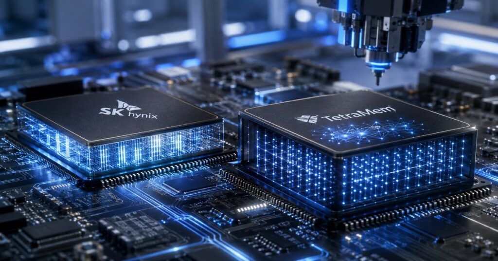
The von Neumann bottleneck has been a known problem in computing for seventy years. The solution has proven elusive because it requires rethinking not just how chips are designed but how memory and computation relate to each other at the hardware level. A joint research project between SK Hynix and TetraMem has produced the most complete demonstration yet of what that solution looks like when it works: an AI System-on-Chip built on memristor technology that performs the core mathematical operations of AI inference directly inside the memory cells where the model weights live, without shuttling data back and forth to a separate processor.
The memristor-based AI SoC, built around TetraMem’s MX100 architecture, is designed to handle depthwise convolution — a fundamental operation used heavily throughout modern AI inference workloads — in an analog in-memory computing framework. The research demonstrates multiple orders of magnitude improvement in energy efficiency compared to conventional GPU-based inference architectures, and represents the first fully integrated memristor/CMOS computing chip of its kind to reach a production-viable design.
KEY DEVELOPMENTS
- SK Hynix and TetraMem announced a joint research breakthrough: a memristor-based AI System-on-Chip (SoC) that performs depthwise convolution — a fundamental AI inference operation — directly inside memory cells rather than shuttling data to a separate processor.
- The TetraMem MX100 SoC, built at the 65nm technology node, integrates ten neural processing units (NPUs) with 8-bit memristors, a RISC-V CPU, and 1.5MB of on-chip SRAM in a fully integrated chip — the first of its class to combine memristor/CMOS computing in a production-grade package.
- In-memory computing eliminates the von Neumann bottleneck: the power, latency, and bandwidth cost of moving AI model weights between memory and processor is eliminated when computation happens where the data lives.
- As foundation models scale toward trillions of parameters, this architecture offers a potential path to dramatically lower power consumption and hardware costs for AI inference at scale.
What the Breakthrough Is
The Von Neumann Bottleneck Explained
Every modern computer, from a smartphone to a data centre GPU, is built on the same fundamental architecture: processors compute, memory stores, and data moves back and forth between the two over buses and interconnects. That movement is not free. It consumes power, takes time, and at the scale of a modern AI inference workload — where a frontier language model may have hundreds of billions of parameters that must be loaded repeatedly into processor registers during each forward pass — the data movement cost dominates the total power budget of the system. At current GPU efficiency levels, the energy consumed moving model weights from memory to processor is often greater than the energy consumed performing the actual matrix multiplications that constitute the model’s computation.
What In-Memory Computing Does Differently
Memristor-based in-memory computing eliminates the separation between storage and computation by performing matrix-vector multiplications — the dominant mathematical operation in neural network inference — directly within the memory array. Rather than reading a weight value from a memory cell and sending it to a multiply-accumulate unit in a distant processor, the crossbar array of memristors performs the multiplication using Ohm’s Law and Kirchhoff’s Current Law directly in the physical medium of the memory itself. The result is computed at the point of storage. No data movement is required for the core arithmetic. The TetraMem MX100 SoC extends this principle to depthwise convolution — the operation used in efficient neural network architectures like MobileNet and EfficientNet — with one of its ten NPUs specifically optimised for that computation pattern. The chip also integrates a RISC-V CPU for on-chip program execution and a DMA engine for rapid internal data transfer.
Why SK Hynix’s Involvement Matters
SK Hynix is not a passive research partner in this collaboration. The company is the world’s dominant supplier of high-bandwidth memory, the vertically stacked DRAM that sits directly alongside Nvidia’s GPU accelerators in every major AI server. It controls approximately 60 percent of the HBM market and reported revenue near ₩52.6 trillion in Q1 2026 — its first quarter above ₩50 trillion and up close to 200 percent year over year. The company’s multiyear technology partnership with Nvidia, announced earlier this year, has cemented its position as the primary memory supplier for the current AI infrastructure buildout. That position makes SK Hynix’s investment in memristor-based in-memory computing particularly significant: this is not a startup bet on a speculative technology. It is the company that profits most from the current AI memory architecture investigating whether the next architecture eliminates the bottleneck its current products are designed to serve. If in-memory computing works at scale, the demand for conventional HBM as a data-movement buffer changes. SK Hynix is making sure it is on both sides of that transition.
The Backstory: Why This Approach Has Struggled to Scale
Memristor-based computing has been a research category for decades, with early excitement in the 2010s followed by a prolonged period of limited commercial progress. The technical challenges are real: analog memory cells are inherently noisy compared to digital binary storage, weights stored in memristors drift over time, device-to-device variation creates inference accuracy problems at scale, and the programming precision required for reliable 8-bit inference in a crossbar array has been difficult to maintain across large-scale chips. TetraMem’s MX100 SoC represents a significant engineering advance in addressing those challenges: it achieves 8-bit memristor precision in a fully integrated chip at the 65nm technology node, a combination that previous academic demonstrations and smaller-scale prototypes had not achieved in a production-viable form.
The 65nm node is not a leading-edge process; modern digital chips are manufactured at 3nm and below. The advantage of targeting 65nm for in-memory computing is that it is a mature, well-understood, and cost-effective process, which matters for a chip architecture that is itself novel. You do not want to combine a new chip architecture with a new manufacturing process; the TetraMem MX100’s use of 65nm lets the team isolate the memristor/CMOS integration challenges from the manufacturing challenges that leading-edge nodes introduce.
What It Means for AI Inference Economics
The energy cost of AI inference has become one of the industry’s most closely watched operational variables. As covered in our analysis of the energy and water footprint of AI at scale, the current trajectory of AI inference power consumption — driven by growing model sizes and increasing request volumes — is on a path that strains both power grid capacity and corporate energy cost structures. In-memory computing offers a pathway to dramatically lower energy per inference operation, not through incremental optimisation of conventional GPU architectures but through a fundamental change in how computation relates to data storage. The specific improvement magnitude depends heavily on model architecture, workload characteristics, and the specific task being run. Depthwise convolution workloads, which are the focus of this SK Hynix–TetraMem demonstration, are particularly well-suited to in-memory computing acceleration because their memory access patterns are highly regular and their arithmetic operations map cleanly onto the matrix-vector multiplication that crossbar arrays compute naturally.
The Limits of What This Announcement Represents
Honest analysis of this breakthrough requires acknowledging what it does not yet prove. The MX100 SoC demonstrates in-memory computing for a specific, well-defined operation at a specific scale using a mature manufacturing process. Scaling the approach to the trillion-parameter models that represent the current frontier of AI development requires solving additional challenges: the crossbar array size limitations that constrain how large a model can be represented in a single in-memory chip; the precision requirements for transformer attention operations, which are more complex than convolution; and the system integration questions around how an in-memory compute chip communicates with the rest of a server architecture. None of these challenges are insurmountable, but they are non-trivial, and the research community has repeatedly seen in-memory computing results that were impressive in controlled benchmarks prove difficult to translate into general-purpose AI acceleration.
What Happens Next
The SK Hynix–TetraMem collaboration points toward a research roadmap rather than an immediately deployable commercial product. The next milestones to watch are evidence of the approach working with transformer-based model architectures rather than convolution-based ones, and demonstrations of multi-chip integration that would allow larger models to be distributed across arrays of in-memory compute units. SK Hynix’s Nasdaq ADR listing, scheduled for July 10, 2026, will give the company access to US equity markets, additional capital, and greater visibility for partnerships with US AI labs that might accelerate the translation of this research into production hardware. The longer timeline question is whether in-memory computing matures fast enough to compete with the conventional GPU architecture trajectory before Nvidia’s next two or three hardware generations further entrench the current paradigm.
Why It Matters
The SK Hynix–TetraMem result matters as a proof of concept rather than a product. It demonstrates that memristor-based in-memory computing can achieve 8-bit precision in a fully integrated chip capable of handling real AI inference operations at a level of integration that previous work had not reached. If the approach scales, it represents not an incremental improvement on the current AI hardware stack but a potential architectural discontinuity — a shift from moving data to computation toward performing computation where the data lives, with fundamentally different power and latency characteristics than any GPU generation can deliver. The companies that prove this architecture at scale will control one of the most valuable intellectual property positions in the next decade of AI infrastructure.
Sources
TetraMem MX100 SoC research documentation and arXiv pre-publication (arXiv:2410.14882). Advanced Intelligent Systems (Wiley Online Library). SK Hynix AI research and HBM market data (news.skhynix.com). NVIDIA–SK Hynix partnership announcement (nvidianews.nvidia.com), June 2026.